Comprehensive analysis of the market prospects for glass - based chip substrates, covering technology, applications, regional competition, and future trends!
01 Market Drivers
1.1 Requirements for Technological Upgrades
•5G/6G Communication: High - frequency signal transmission demands that substrate materials have low dielectric loss and high signal integrity. Glass Core Substrates have emerged as an ideal alternative to traditional organic materials.
•AI and High - Performance Computing (HPC): The improvement in chip computing power drives the demand for advanced packaging (such as 3D IC). The excellent heat dissipation and dimensional stability of glass substrates can support a higher - density chip integration.
•The Slowdown of Moore's Law: As semiconductor processes approach the physical limit, enhancing performance through packaging technologies (such as Chiplet) has become a trend. Glass substrates have significant potential in this area.
1.2 Expansion of Application Scenarios
•Consumer Electronics: The demand for thinner, lighter, and highly integrated products in smartphones and AR/VR devices continues to grow.
•Data Centers and Cloud Computing: There is a surging demand for high - bandwidth and low - latency substrates in high - speed optical modules and AI servers.
•Automotive Electronics: Autopilot (L4/L5) and electrification drive the demand for highly reliable substrates in vehicle - mounted sensors and domain controllers.
02 Technological Development Trends
2.1 Material Innovations
•Optimization of Glass Formulations: Thermal stability and mechanical strength are enhanced by adjusting the glass composition (such as low - coefficient - of - thermal - expansion glass).
•Hybrid Substrate Technology: Combining glass with organic materials (such as glass + ABF film) to balance performance and cost.
2.2 Advanced Packaging Processes
•2.5D/3D Packaging: The application of glass substrates in Through - Silicon Via (TSV) and Microbump technologies is accelerating.
•Optoelectronic Integration: The potential of glass substrates in the packaging of optical communication chips (such as Co - Packaged Optics, CPO technology).
2.3 Breakthroughs in Manufacturing Processes
•Laser Drilling and Micro - processing: Improving the high - precision processing capabilities of glass substrates and reducing costs.
•Large - scale Production: With the maturity of equipment (such as large - size glass substrate production lines), the unit cost is expected to drop by more than 30%.
03 Regional Competitive Landscape
3.1 The Asia - Pacific Region Takes the Lead
•China: Domestic manufacturers (such as Dongshan Precision and Shennan Circuits) are accelerating their strategic layout. Policy support (such as the "14th Five - Year Plan" for electronic materials) is promoting domestic substitution.
•Japan and South Korea: Enterprises like Sumitomo Chemical and Samsung Electro - Mechanics lead in technology in the field of high - end glass substrates, focusing on the automotive - grade and server markets. •Taiwan, China: Large packaging manufacturers such as Taiwan Semiconductor Manufacturing Company (TSMC) and ASE Technology Holding Co., Ltd. are promoting the implementation of glass substrates in advanced packaging.
3.2 Europe and the United States Catching Up
•The United States: Intel and Corning are collaborating to develop glass substrate technology, targeting data center and military applications.
•Europe: Focusing on automotive electronics (such as Bosch and Infineon), it is promoting the application of glass substrates in scenarios requiring high temperature resistance and high reliability.
04 Main Challenges
4.1 Cost Pressure
The initial production cost of glass substrates is higher than that of traditional organic substrates (such as BT resin), and cost reduction relies on large - scale production.
4.2 Technical Barriers
The processing difficulties caused by the brittleness of glass (such as cutting and via filling) still need to be overcome.
4.3 Supply Chain Risks
The supply of high - purity glass raw materials (such as quartz sand) depends on a few manufacturers (such as Nippon Electric Glass), and there are geopolitical risks.
05 Future Outlook
5.1 The Critical Window from 2025 to 2030
•Increase in Market Penetration: It is expected that the penetration rate of glass substrates in the advanced packaging market will increase from 5% in 2025 to over 20% in 2030.
•Cost Inflection Point: After 2027, the scale effect will become apparent, and the cost of glass substrates is expected to be on a par with that of high - end organic substrates.
5.2 The Outbreak of Emerging Applications
•Photonics Chips: The potential of glass substrates in optical interconnection and quantum computing remains to be unleashed.
•Space Electronics: The radiation - resistant and high - temperature - resistant characteristics meet the needs of satellite and deep - space exploration.
5.3 Reconstruction of the Industrial Chain
The full - chain collaboration from materials (glass manufacturers), equipment (laser processing machines) to packaging factories will become the core of competition.
06 Conclusion
6.1 The market for glass-based chip substrates is expected to witness structural growth in the coming decade. Technological breakthroughs and large-scale production will serve as the core driving forces.
6.2 In the short term, it is necessary to surmount the bottlenecks in cost and processing technology. In the long run, its irreplaceability in fields such as high-performance computing and optoelectronics will reshape the landscape of the semiconductor packaging industry.
6.3 It is advisable to keep an eye on manufacturers that possess material research and development capabilities and are closely tied to leading customers (such as enterprises in the supply chains of Corning and Taiwan Semiconductor Manufacturing Company, TSMC).
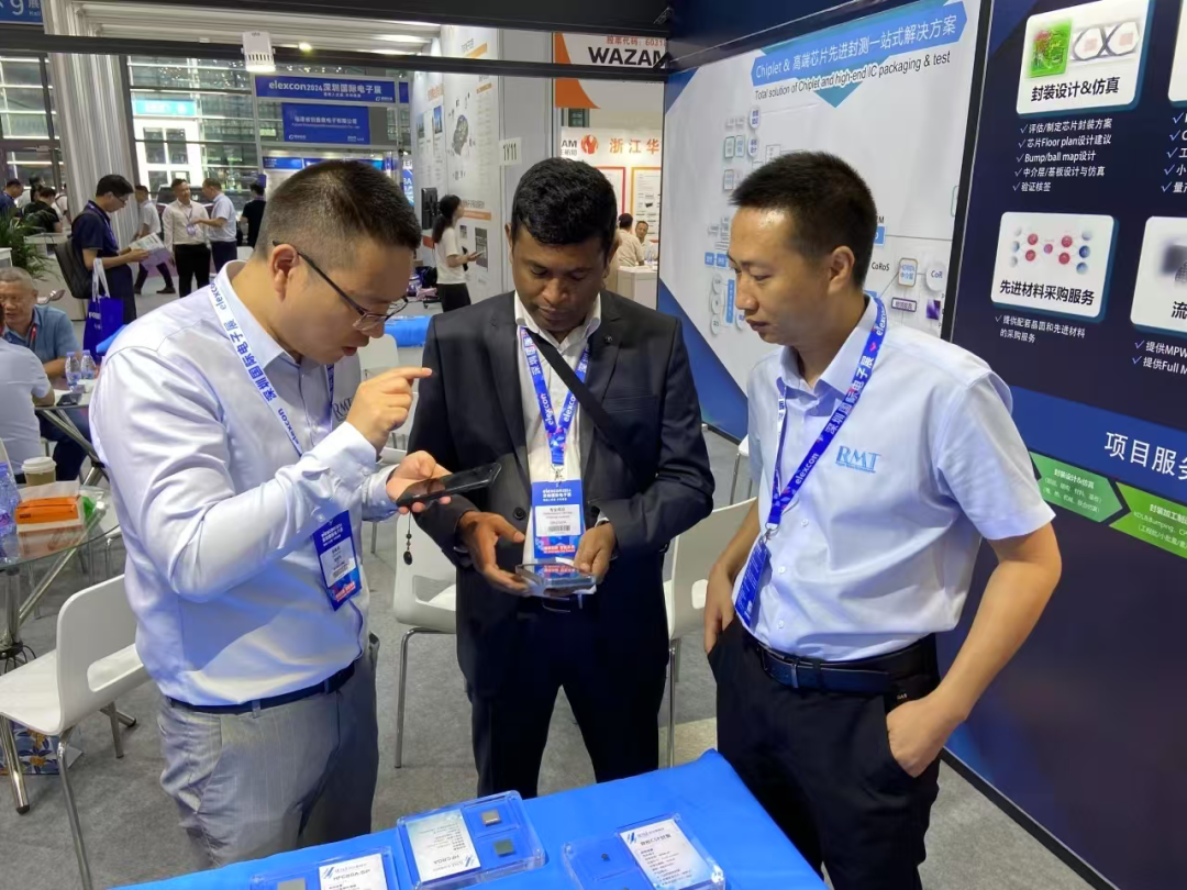
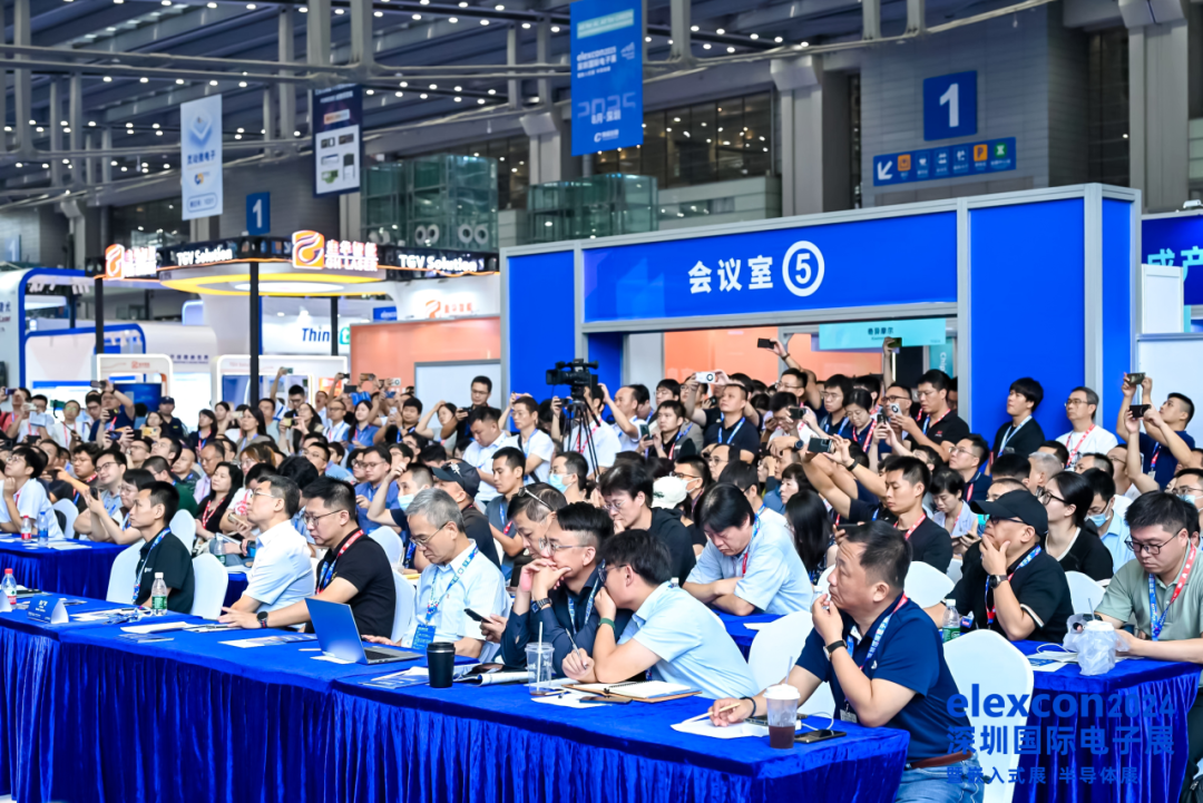
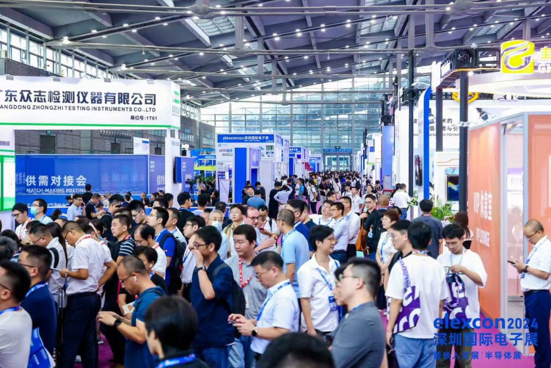
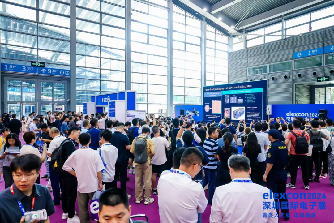
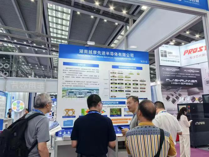
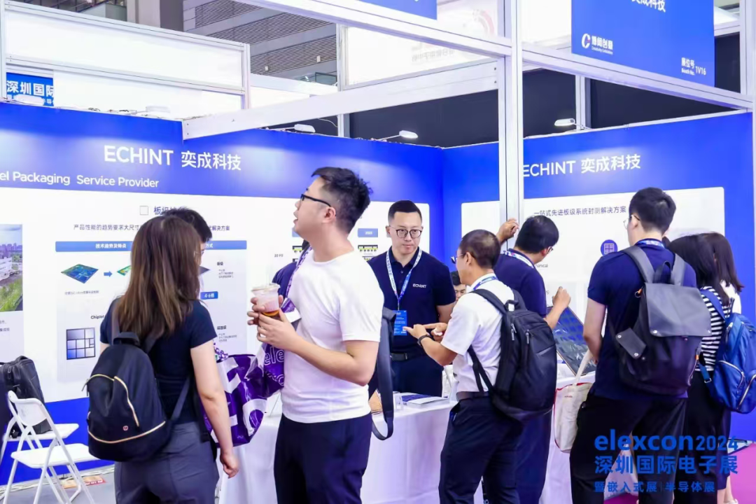
In 2024, the elexcon Semiconductor & SiP China Conference was held around the four themes of "Heterogeneous System Integration Applications", "Heterogeneous System Integration Manufacturing", "Heterogeneous System Integration Implementation", and "Key Processes of TGV Glass Substrates". 41 industry experts and representative enterprises brought more cutting - edge technologies and market reports to the industry. A total of 1,837 professional audiences and 3,050 person - times attended the conference. The "SiP/Chiplet/Heterogeneous Integration Ecosystem" and "TGV Process of Glass Substrates" set up at the venue attracted nearly 100 well - known industrial enterprises to exhibit, providing an advanced technical platform for industry professionals to comprehensively understand the optimal solutions of the upstream and downstream industrial chains, conduct business negotiations, and have in - depth exchanges and discussions on the future development of the industry and the implementation of business.

In 2025, we will continue to promote the development of the advanced packaging industrial chain. In the era of AI, we will focus on the technological routes of advanced packaging such as 2.5D/3D/TSV/PLP/RDL and other processes, the improvement of assembly technologies for packaging process equipment, advanced materials and interconnection technologies, the TGV (Through Glass Via) process and material optimization solutions. We will once again showcase to the industry the new technological directions of the advanced packaging industrial chain and the achieved results of the technological advancement and implementation of the glass-based carrier board industrial chain.